Transparent Encoding Overview
Transparent Encoding Applications and Support Overview
Transparent mode is for unique applications that require the data and clock signals to be sampled at one end of a circuit and replicated at the far end. For example, applications in which:
Data rates are low (32 Kbps or less) and rates can vary over time. The sampling jitter prevents use of higher data rates.
Data rates are low and fixed and/or low network latency is required.
Clocks must disappear (transitions stop) periodically during circuit operation.
The transparent encoding scheme is supported only when you have worked with the Juniper Networks Technical Assistance Center (JTAC) to verify that your application requires this encoding scheme. You may need to use special adapters on the cable to properly map the data and clock signals to the connector pins that the application uses.
We recommend that you do not use transparent encoding in WAN environments because of its large consumption of bandwidth.
How Basic Transparent Encoding Works
There are two modes of transparent encoding. They are Transparent 4 mode (TRANS) and Transparent 8 mode (TRANS8). Transparent 8 mode is supported only on CTPOS release 6.4 and later.
Transparent encoding mode 4 samples incoming data on four input signals (SD, TT, RTS, and DTR), transports these signals across the IP network to the remote end of the circuit, and sends the signals on four output signals (RD, RT, CTS, and DSR). Figure 3 shows a simplified model of a transparent encoded circuit.
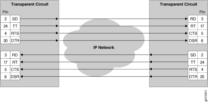
The signal sampling rate is based on the configured port rate. For example, if the port rate is 128 Kbps, then the four signals are sampled at 128 KHz, which generates a packet flow through the IP network of 512 Kbps (4 x 128 KHz). The smallest sampling rate available is 5.3 μsec (approximately 192 KHz).
To prevent errors in transport, both ends of the circuit must be synchronized with each other. You can achieve synchronization either by locking each CTP node to a common reference or by enabling adaptive clocking on one end of the circuit.
Transparent 8 encoding is an extension of Transparent 4 encoding. Compared with Transparent 4 encoding, which sends four signals in each direction, Transparent 8 encoding doubles the bandwidth and allows eight signals to be sampled and transported. This allows signals to be sent from additional interfaces that were not supported in Transparent 4 encoding, although the bandwidth usage will be higher.
Using Phase-Correction FIFO Buffer with Transparent Encoding
The transparent encoding feature provides a phase-correction FIFO buffer. This FIFO buffer aligns the clock and data phase relationship on a transparent encoded circuit in which the clock travels in one direction through the network, and the data travels in the opposite direction. The transparent FIFO buffer is needed because of the latency of signal transport over the IP network.
Figure 4 shows the phase-correction FIFO buffers. You can enable the phase-correction FIFO buffer at either end of the circuit. You would not enable the FIFO buffer at both ends of the circuit.
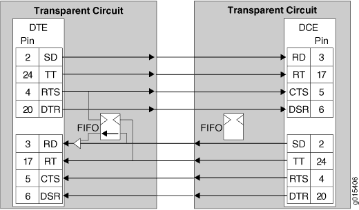
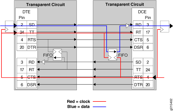
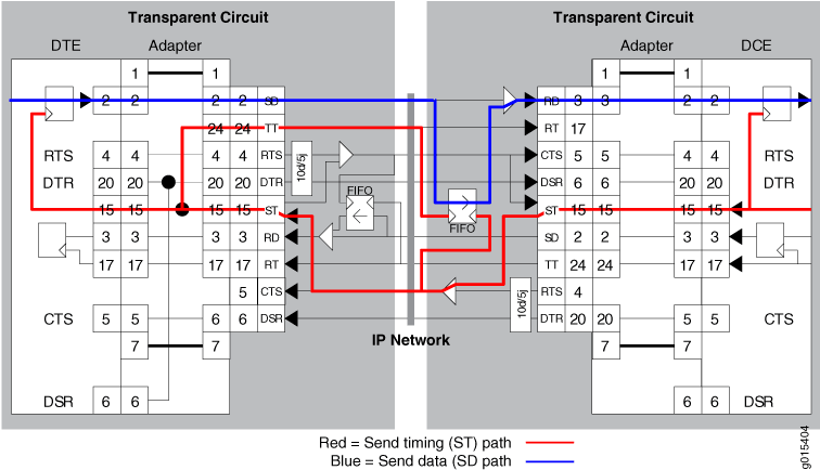
Figure 5 shows the paths of the clock and data through the phase-correction FIFO buffer that is enabled on the transparent circuit on the right.
The clock enters the network from the DCE, goes to the DTE, and then clocks data into the network on the DTE. The clock is also looped back on the DTE to enter the network in phase with the data as it travels from the DTE to the DCE.
The data enters the FIFO buffer in phase with the clock passing through the network from the DTE to the DCE, while data is clocked out of the FIFO buffer with the clock that entered the network from the DCE, which is in phase with the user clock.
Like in TRANS encoding, you can use the 16 bit phase correction FIFO in TRANS 8 encoding to accommodate the problems that can be caused by the high latency in the circuit whether or not the remote DCE device can accept TT input or not.
When the customer DCE device can support the TT signal returned by the DTE, the phase correction FIFO is not needed. The DCE transmit clock (ST) is sampled and carried downstream to the DTE, where it is used to generate the upstream data that is sent back to the customer DCE. This clock data is also sent as the DTE transmit clock (TT) to travel along with the data in phase. When these signals get back to the customer DCE device, they are still in phase (same delay through the network), so the customer DCE can use the TT signal to recover the transmit data on the SD lead.
Consider a scenario in which the customer's upstream DCE does not use the TT signal for capturing upstream data, and instead uses the ST clock. Here, due to the latency of the ST clock traveling downstream and the time taken for the return trip of the data, it is difficult to ensure error-free data transport. In such a scenario, you can use phase correction FIFO to ensure error-free data transport.
The SD or TT clock and data signals get back to the upstream CTP device, where the data is clocked into the FIFO using the TT clock, which is in phase. This data is clocked out of the FIFO using the upstream ST clock, and the data is realigned to be in phase with the ST clock.
Using Send Timing (ST) Clocking for Higher Speed Circuits with Transparent Encoding
When the relationship between the clock and the data signals is critical, you can use ST clocking with transparent encoding to prevent delay and jitter in CTP2000 series devices, making it possible to carry higher speed circuits in transparent mode.
Figure 6 shows the issue of delay and jitter where a transparent encoded circuit connects a DCE to a DTE. The circuit is set up as follows:
The high-speed clock and data lines (shown in red) are aligned by a FIFO buffer at the DCE.
The signaling leads (shown in blue) are passed end-to-end without going through the FIFO buffer. The signaling paths that carry non-timing-critical signals are subject to delay and jitter.
The problem is that when a FIFO buffer is used at one end of the circuit, an additional clock path from the DCE to the DTE is needed to carry a clock to the DTE so that it can return a DTE-to-DCE clock that is in phase with the data. This DTE-to-DCE clock is needed to clock the FIFO input. Normally, one of the signal lead paths carries this transmit clock. However, when the circuit is running at speeds above 32k, the delay and jitter on these paths make these signal choices nonoptimal.
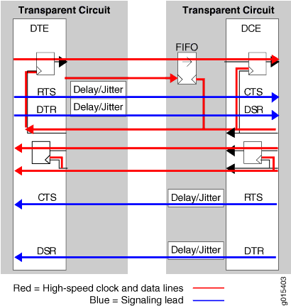
To solve the issue of delay and jitter associated with the signaling leads, you can use the ST interface signal to feed or sink the RTS-to-CTS signal path. By using the ST interface signal instead of the RTS-to-CTS signal path, delay and jitter are removed from that signal path. Figure 7 shows a transparent-encoded circuit with the additional ST functionality:
At the DCE, the RTS-to-CTS signal path is configured to use ST (as an input from the DCE) to feed that signal path through the network.
At the DTE, that signal is placed onto the ST lead, which is configured as an output.
When you configure transparent encoding to use the ST lead instead of RTS/CTS, you can specify whether or not ST is an input lead.